
Key Features of PCB Boardsv
PCBs are the basis for many of our modern devices and everyday electronics. From security cameras to smoke detectors, motion sensors and even electronic door locks, PCBs play a role in many different types of equipment. But what exactly are the key features of a pcb board?
Printed circuit boards have copper on both sides, or external layers, with insulating materials sandwiched in between. The simplest PCBs are two-layer boards, while more complex ones have multiple internal layer structures that allow for greater routing options and provide shielding from electromagnetic interference (EMI) and power supply decoupling.
The design process starts with schematic capture and simulation, where graphical symbols of components are used to build the circuit topology. Detailed circuit modeling allows designers to identify potential problems before they become physical issues during manufacturing. This step can save time, money and frustration for both the designer and the manufacturer, as it can prevent rework or scrapping of costly components that were incorrectly placed on the board.
Once the design is complete, a software program called ECAD (Electronic Computer Aided Design) is used to create a PCB layout. Once the design is ready, it is sent to a fabrication house where bare laminate is covered with photosensitive film that is imaged (sensitized) using light exposure, leaving only the areas that are to be plated with copper.
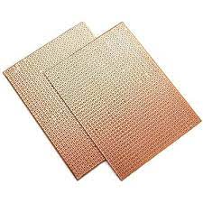
What Are the Key Features of PCB Boards?
The exposed areas are then bathed in copper ions to form the desired pattern of holes and traces. The resulting pcb is inspected and evaluated for errors, such as traces that touch each other or drill holes that are too skinny to be properly drilled. A DRC – design rule check – is also performed, which checks the design for errors and provides the opportunity to resolve them before production.
Resistors are the most common PCB component, absorbing electric current and dissipating it as heat. Capacitors are the second most common, holding electrical charge and releasing it when needed elsewhere on the circuit. Transistors amplify the charge on a circuit board to switch or control its electrical signals, and can be made in a variety of shapes and sizes. Inductors are similar to capacitors, storing energy as a magnetic field when an electric current passes through them.
Solder paste is applied to the surface mount pads on a circuit board and then heated during the reflow process to melt it, creating an electrical and mechanical connection between the pad and the component. The circuit board can then be tested for electrical continuity, solder strength and other characteristics.
A pcb that fails during assembly or use can result in loss of data, damage to the internal components and a reduction in performance. In order to ensure quality, a PCB should be designed with high-quality materials and a tight tolerance of dielectric spacing. This ensures better mechanical properties, less expansion and warpage, as well as lower electrical characteristics such as impedance variations. This results in better reliability and a safer working environment for users.

